I2C Communication Pull up resistor calculation with LTspice Simulation:
I2C Communication:
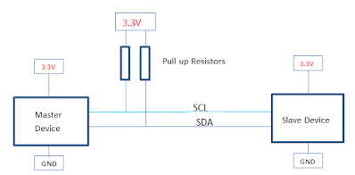
This post rewind the I2C Hardware overview, I2C Pullup resistor value calculation, and LT Spice simulation.
Hardware Overview:
- The I2C bus is a very popular and simple bus used for communication between a master or multiple masters and single or multiple slave devices.
- This communication only uses two-wire SDA and SCL. Which is a serial data line and serial clock line.
- Both SCL and SDA lines are open-drain or open-collector configurations. This means it needs an external pullup resistor is completely taking control of generating the logic high signal.
- I2C uses an 8-bit data structure which is a common data format for most Microcontroller and Microprocessor
- In the 8 bit communication, 7 bits are address bits and the last bit represents the Read/Write operation (1=Read Write =0)
- I2C Protocol is address-based, meaning that all the slave IC must have a unique address, this address is configured through hardware pins to logic "1" or "0". Some slaves may not have address pins and they have a static internal address that cannot be changed.
I2C Operating modes:
The above-given parameters are used to select the Pullup resistor values.
- I2C standard specifies the maximum bus capacitance for each mode of operation. This includes the Parasitic capacitances on the bus due to the traces.
- The total amount of bus capacitance C bus is limited in the I2C Communication for each mode of operation
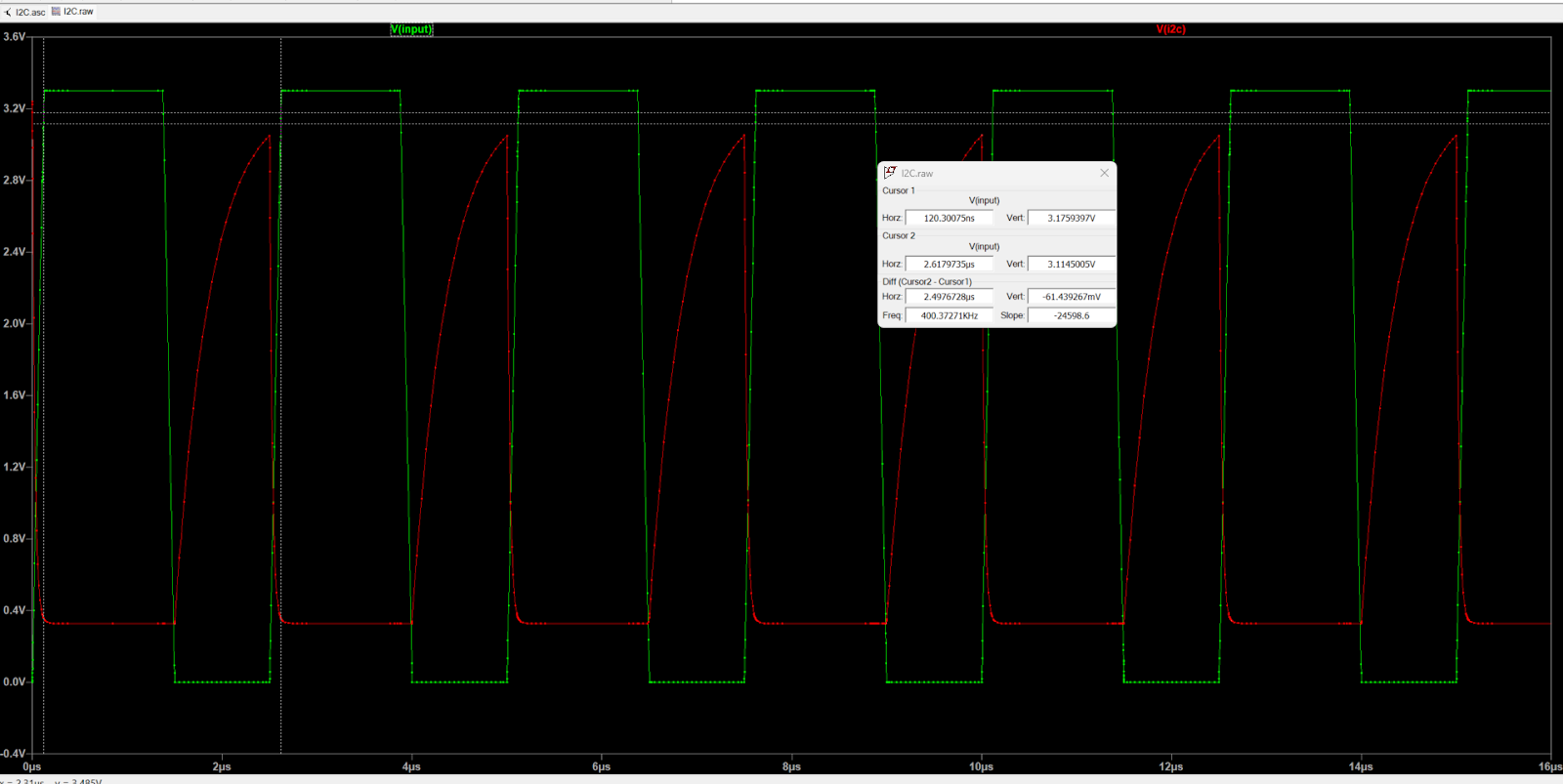
- In order to meet the timing requirements for the mode of operation used, we need to be within the maximum rise time specification.
- The Maximum rise time is controlled by the RC time constant created by the pull-up resistor value. and is defined as the amount of time it takes to transition from VIL to VIH
VOL: Nominal voltage
corresponding to a low logic
state at the output of a logic
gate
VOH: Nominal voltage
corresponding to a high logic
state at the output of a logic
gate
VIL: Maximum input voltage that
will be recognized as a low
input logic level. (0.3*VCC)
VIH: Minimum input voltage that will
be recognized as a high input
logic level. (0.7*VCC)
(Datasheets for the digital parts will contain electrical specifications for logic threshold, those voltage levels that represent a logic "1" or "0"
There will be specifications for output (What the chip generates to represent "0" or "1")and Inputs (What the chip will read as "0" or "1"
Outputs are often called VOH and VOL
Inputs are often called VIH and VIL)
Formulas:
R pull-up max = Trisemax / 0.8473*C bus
R pull-up min = VCC-VOLmax / IOLmin
Example :
Input :
I2C communication Mode: Fast mode 400Khz
I2C Total bus capacitance: 200pF (Including PCB trace Capacitance)
Vcc: 3.3V
From the I2C Specifications, we know Rise time for Fast mode is 300ns, VOL-max: 0.4V, and IOL: 3mA
Rpullup affects VOL :
We have calculated the Rmin, because if the resistance is too low ( meaning pull-up current is too strong) then the VOL could potentially be higher than the VIL of the input buffer. thus it could not detect logic low properly. The low limit of the pull-up resistor is a function of the drain to source resistance of the FET while ON(RDS_ON) and the pull-up resistor.
Some real-time debugging steps:
- Make sure that while probing the SCL and SDA wave shapes are Square
- Make sure the Master and Slave devices voltage and Ground levels are proper
- Frequency and rise time (Slow rise time)
- Improve the rise time, Decrease the pullup resistor value
- If Pullup is too low excess current will flow through the lines and it may damage the component.


Comments
Post a Comment